Prometheus is my most complicated (so far) hardware design. It has been done for Matay in 2000. It is a bridge joining traditional asynchronous Zorro III Amiga expansion bus with standard PCI. It allows for using PCI expansion cards in Amiga 3000 and 4000. Unfortunately only 250 boards have been produced. Thanks to agreement of all parties involved, the design can be opened to the public.
 Prometheus PCI Bridge by Grzegorz Kraszewski is licensed under a Creative Commons Attribution-NonCommercial-ShareAlike 3.0 Unported License. All files and archives available on this webpage are covered by this license.
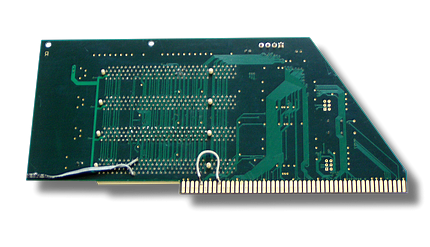
Prototype rev. B
This is the first working version of the Prometheus. There were only two rev. B prototypes built. Both were assembled manually, so there are no SMD components. PLD chips are socketed, they were removed for every reprogramming. As PLCC-84 was the biggest easy to socket package available, the design had to be splitted into 3 chips, to deliver sufficient number of I/O pins. The chip with a sticker "L" handles lower 16 bits of address and data, chip "C" is the control chip, chip "H" (without a label) handles upper 16 bits. While it is an early prototype, it already uses 4-layer PCB to get proper impedances of tracks carrying PCI signals, running over inner ground and +5 V layers. The second rev. B prototype has been sent to Picasso 96 authors for developing Voodoo 3 driver, about October 2000. It can be seen on the bottom side, that rev. B needed a few fixes...
Prometheus prototype rev. B, top view.
Prometheus prototype rev. B, bottom view.
Prototypes rev. C and D
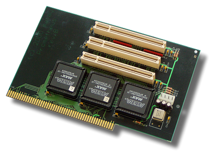
While revision B of Prometheus was a proof of concept and developer board for drivers, rev. C has almost the same appearance and shape as the final rev. E product. It was assembled and soldered automatically, so most of components are SMD ones. Two bigger capacity (EPM 7128 instead of EPM 7064) chips in PQFP-160 packages delivered enough I/O pins. The revision C had some bugs in PCB layout, that is why revision D followed. Unfortunately it seems no single rev. C board survived. I have one rev. D with the last bug fixed by wires. This last bug were missing PCI interrupt lines. I've had to fix it very fast, as rev. D Gerber files had been already sent to a PCB manufacturer. Fortunately I've sent the fix on time, so the final product has working interrupts. You can see below the revision D prototype and a close-up of wires soldered directly to leads of a chip in PQFP package. These leads have 0.635 mm raster, and soldering them by hand was not easy, but it worked. One can also notice that 32.768 MHz quartz oscillator was used instead of 33.000 MHz, but PCI cards had no objections. Of course production run had 33.000 MHz oscillators.
Prometheus prototype rev. D, top view. Red interrupt wires
taped to the PCB.
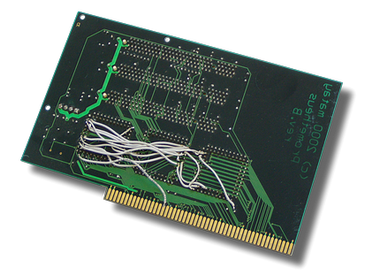
Prometheus prototype rev. D, bottom view. Some cables left,
used for testing.
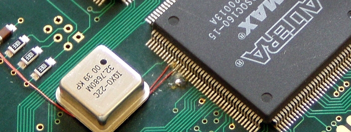
PCI interrupt lines wired directly to a chip in the rev. D prototype.
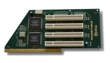
The Final Version (rev. E)
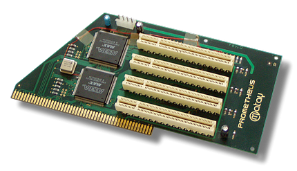
The final revision E of Prometheus has interrupts routed on the bottom side. All 250 boards were produced in a single batch, all using exactly the same components. From those 250 boards only two did not pass the quality control. One of them was fixed as it turned out that oscillator was soldered rotated by 180 degrees (oscillators and PCI slots were inserted manually before automatic soldering). All the boards were tested by inserting 4 PCI cards in all the slots (one of them was Voodoo 3), mounting the Prometheus in an Amiga 4000, then booting into Workbench running on Voodoo. Finally PCIScan tool was started from CLI to check if all the slots work. Printed circuit boards, SMD assembly and soldering of prototypes and of production batch were done in Tele and Radio Research Institute in Warsaw.
Prometheus final rev. E, top view.
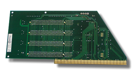
Prometheus final rev. E, bottom view. Board serial number 0048.
High resolution photos of rev. E Prometheus are available in Amiga Hardware Database.
Schematic Diagrams
Below you can find the full schematic diagrams of Prometheus rev. E (production revision). There are two sheets, the first contains PLD chips, Zorro III slot, programming sockets and clock generator. The second sheet contains PCI sockets, PCI lines termination and power supply. Diagrams are available in PDF format, click on the preview to download.
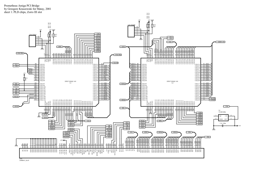
Sheet 1 of the schematic diagram of Prometheus. PLD chips, Zorro III slot.
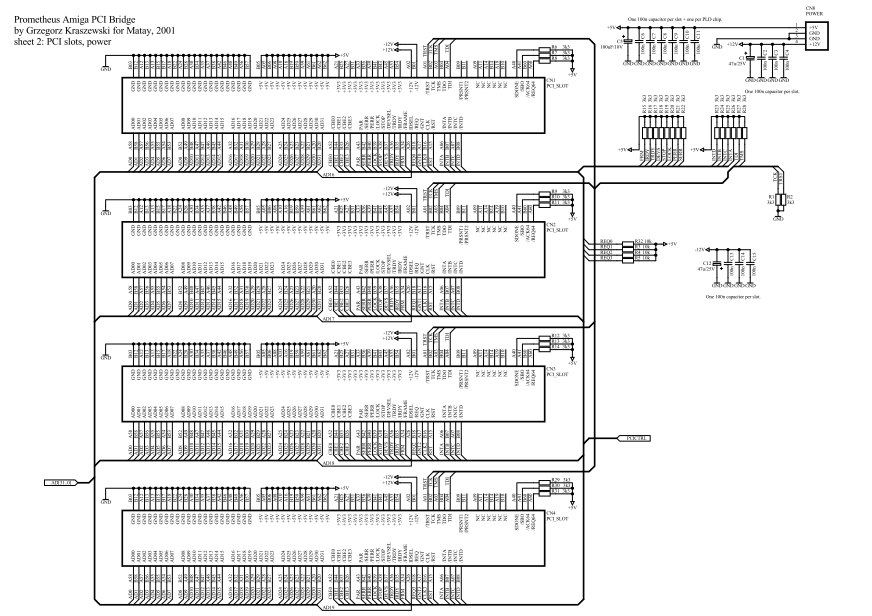
Sheet 2 of the schematic diagram of Prometheus. PCI slots, power.
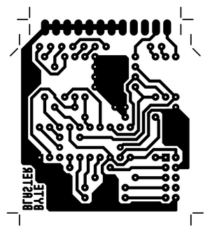
Printed Circuit Board Design
Prometheus printed circuit board has four layers. Two internal layers are power planes (+5 V and ground), all other connections are made on outside layers. The standard track width is 10 mils (0.254 mm). The first three PDF files (linked by bitmap preview images below) are just overviews. Then there is a PDF file with all 13 layers (including soldering masks, SMT paste masks and gold plating masks). Finally there are files in Gerber format (one for each layer and apertures) and drilling file in Excellon format. Exactly these files were sent to the PCB manufacturer.
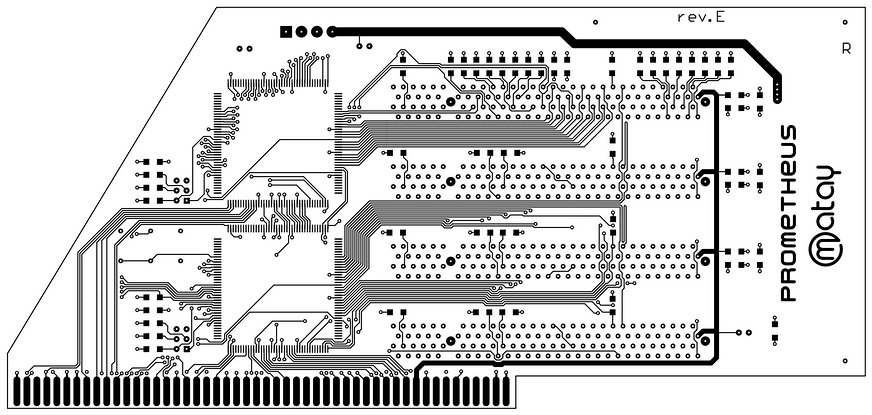
Prometheus board, top layer overview.
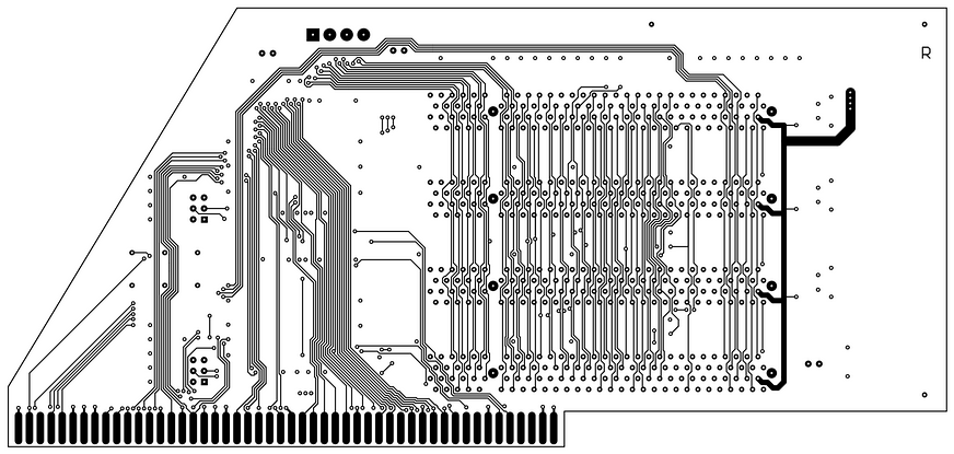
Prometheus board, bottom layer overview.
Prometheus board, top overlay overview.
- top layer.
- bottom layer.
- top overlay.
- top SMT paste mask.
- bottom SMT paste mask.
- top solder mask.
- bottom solder mask.
- ground power plane.
- +5 V power plane.
- board contour.
- mechanical layer.
- top pad master layer.
- bottom pad master layer.
- "BRI_E.APT" – Gerber apertures.
- "BRI_E.TXT" – Excellon drill file.
- "BRI_E.DRL" – binary drill file.
- "BRI_E.GBL" – bottom layer.
- "BRI_E.GBS" – bottom soldering mask.
- "BRI_E.GKO" – board outline.
- "BRI_E.GP1" – ground power plane.
- "BRI_E.GP2" – +5V power plane.
- "BRI_E.GPM" – pads.
- "BRI_E.GTL" – top layer.
- "BRI_E.GTO" – top overlay.
- "BRI_E.GTP" – top SMT paste mask.
- "BRI_E.GTS" – top soldering mask.
Programming Device
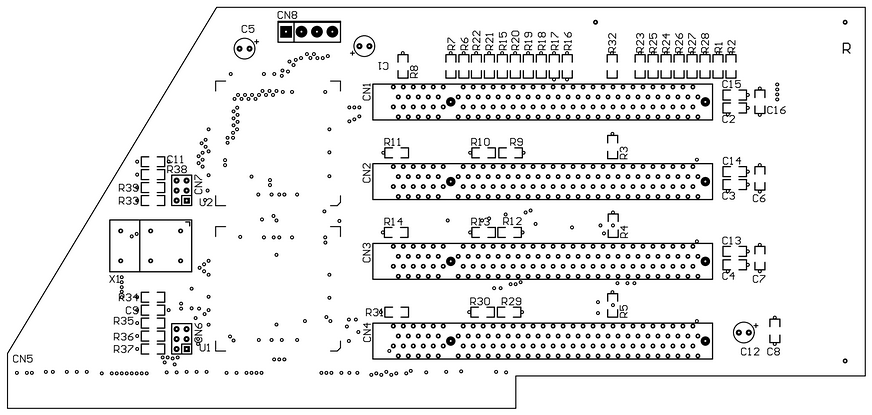
The device is just a homemade version of Altera's ByteBlaster. It connects to a parallel port of a PC. Pins on the edge are used to attach a cable with "programming head" made of 6 pins being inserted into gold plated holes in Prometheus board, labelled as CN6 and CN7. As Prometheus is programmed once, there was no need for a more robust connector, one can be used however. The 74HC244 chip is used as a buffer between a PC and PLD circuit. If something goes wrong, the chip is burned, but not the PC. The 74HC244 is very cheap. In fact one can see on the bottom view photo, that 74HC244 has been replaced after some unfortunate power supply short circuit. One track on PCB had to be replaced by a wire. You can find a schematic diagram of ByteBlaster below, as well as PCB design for the one shown on photos. Schematic diagram image is a link to PDF version.
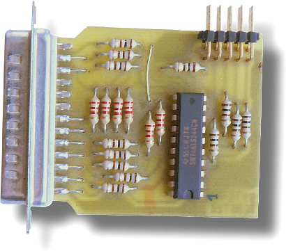
ByteBlaster programming device, top view.
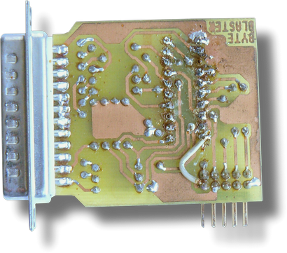
ByteBlaster programming device, bottom view.
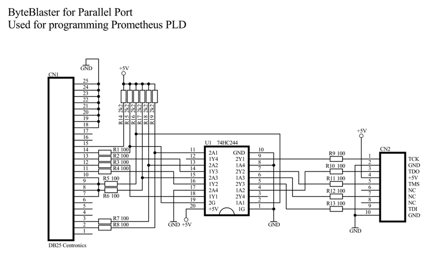
ByteBlaster device schematic diagram.
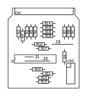
The printed circuit board of the programming device has been designed as one-sided, at a price of three jumpers. Two of them are hidden under the integrated circuit, so not visible on the top view photo. One-sided PCBs are much easier to do at home. For the same reason, all components are mounted through holes. Click on previews below to download PDF versions with 1:1 scale, ready to print vector images. Note that the copper layer is viewed from the top. If one wants to do the PCB with photosensitive emulsion, the printout should be laid with printed side to copper.
ByteBlaster printed circuit board, copper layer.
ByteBlaster printed circuit board, components.
PLD Chips Firmware
Firmware for two programmable logic chips has been designed in Altera's MAX-PLUS II software v10.0. A free version has been used, which has no multichip project feature enabled. That is why there are two separate projects, one for each device. MAX-PLUS II is still available on Altera site, however the project can be also imported into current Quartus II Web Edition. The firmware project archive contains both projects, ready to be loaded to MAX-PLUS II. "PromHigh" project is for chip U1, "PromLow" is for chip U2. Both projects are hierarchical and contain user defined subblocks. For U1 chip, the top hierarchy is prom_ch40.gdf, for U2 it is prom_cl27.gdf. Once the file is loaded, it should be set as hierarchy top level in the application. Most of blocks are logic schematics files, however two blocks, namely Zorro III ConfigROM and the main PCI state machine have been easier to describe with AHDL language (*.tdf files). A scientific paper with a block diagram of the whole device and description of some design ideas may be a nice accompanying lecture.
For those who want just a quick look into the design, I've prepared PDF documents with dumps of all the firmware design files:
Note that all these files contain 40/27 firmware, which was the only one used in the production run. This firmware has no support for PCI-to-PCI DMA transactions, also Prometheus with this firmware is unable to give away PCI busmaster rights. All the needed signals are routed to PLDs however. I've made several more development versions of firmware containing proper bus arbiter and timeout counter. In fact at the end of my work on Prometheus I was able to perform DMA transactions between Realtek RTL8139 network card and Voodoo 3 graphic card, but the work has been aborted. At some later time Michael Böhmer of E3B implemented a new firmware, which is supposed to support DMA between PCI cards.